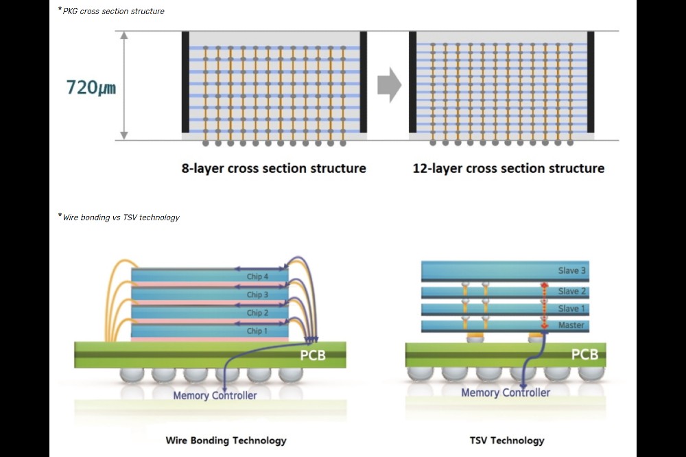
Samsung has figured out a way to stack 12 DRAM chips in the same space it previously only had eight, with the firm leveraging Through Silicon Via technology to achieve the feat.
Despite its current generation high bandwidth memory leveraging wire bonding technology, Samsung has chosen to ditch the method in favour of Through Silicon Via technology. This means that the 12 DRAM chips that make up the layers are bonded through the silicon, with Samsung using more than 60,000 TSV holes in the process.
There are numerous benefits of TSV over wire bonding, and while the ability to cram 12 layers in a space that previously held eight is notable, the technology also enables shorter data transmission time between chips. That means that these new high bandwidth memory chips can achieve faster memory speeds, as well as lower levels of power consumption.
“Packaging technology that secures all of the intricacies of ultra-performance memory is becoming tremendously important, with the wide variety of new-age applications, such as artificial intelligence (AI) and High Power Computing (HPC),” said Hong-Joo Baek, executive vice president of TSP (Test & System Package) at Samsung Electronics.
“As Moore’s law scaling reaches its limit, the role of 3D-TSV technology is expected to become even more critical. We want to be at the forefront of this state-of-the-art chip packaging technology.”
Relying on its 12-layer 3D-TSV technology, Samsung will offer the highest DRAM performance for applications that are data-intensive and extremely high-speed. Also, by increasing the number of stacked layers from eight to 12, Samsung will soon be able to mass produce 24GB high bandwidth memory.
While the technology will be far from cheap, Samsung is hoping that the data centre market will want to benefit from the increased performance that the 12 layers will afford – especially considering the AI arms race that is currently going on in the market.

